Products
High-quality semiconductor materials and equipment for diverse applications
Found 4 products
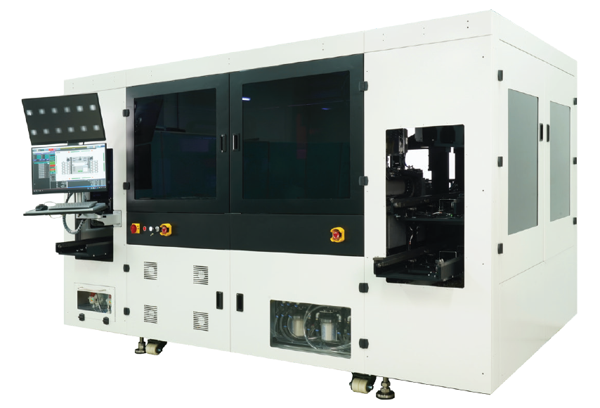
Fully Automated Wafer Scanning Acoustic Tester - PAC (Advanced Package)
Model: 請留言洽詢
▪ Fully Automatic SAT Suite ▪ Multi-probe ▪ Sensor Frequency: 25-200MHz ▪ Scanning Area: 300x200 (mm) ▪ Dimensions: 3200X2000X2150(mm)
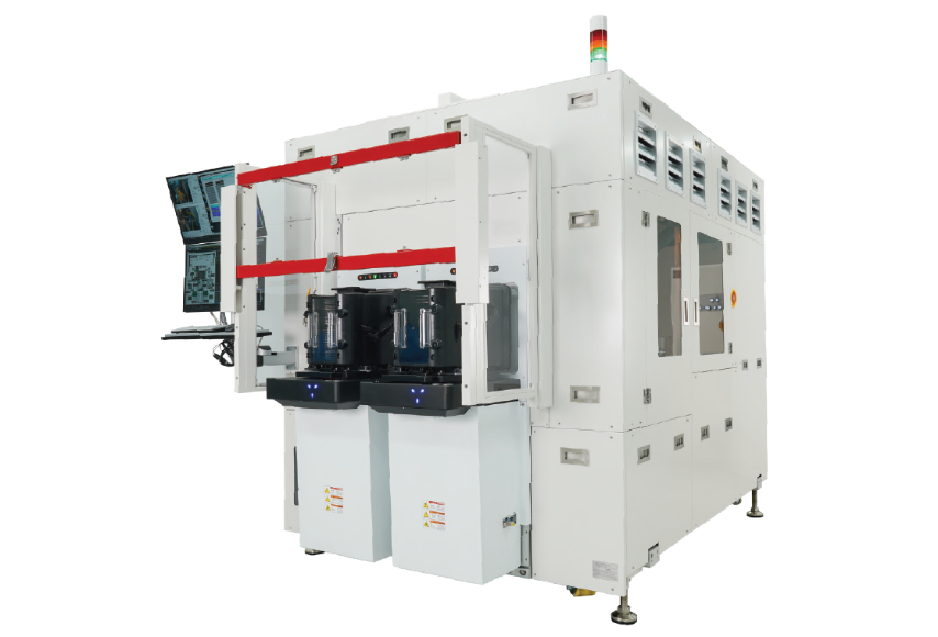
Fully Automated Wafer Scanning Acoustic Tester-W (Wafer)
Model: 請留言洽詢
▪ Fully Automated Wafer Scanning Acoustic Tomography (SAT) ▪ Multi-probe head ▪ Transducer frequency: 50~250MHz ▪ Scanning Area: 300×300mm ▪ Dimensions: 1750×2200×2000mm
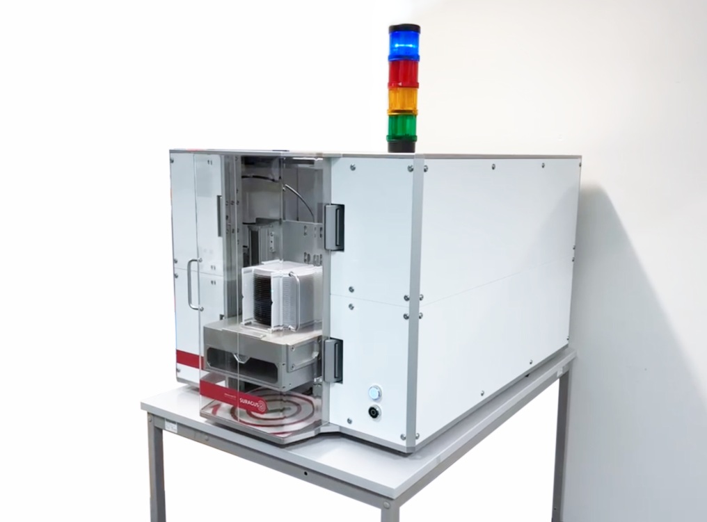
EddyCus® ResMapper
Model: NA
The EddyCus® ResMapper is a fully automated chip imaging device (fully automated model) with an automated chip cassette handling system for full-area characterization of chip substrates or coatings to ensure process reliability and quality assurance in the semiconductor industry. The system is equipped with two non-contact eddy current sensors operating in transfer mode. This allows for highly detailed visualization of the uniformity of the substrate material or conductive coating. This device is typically used for: • Resistivity 0.1 – 100 mOhm-cm, • Board resistivity ranging from 0.0001 – 100,000 ohms/square, • Thin film metal layer thickness ranging from 2 nm to 1 mm, • Total thickness variation ranging from 300 – 1,000 µm and bow pitch ± 1 mm.

Shield sputter
Model: SIGMA1000、CURUS-C200、H-VAM
Nowadays, Electro-Magnetic Interference (EMI) Shield in the mobile device is raised as an critical issue according to the increase of semiconductor package in the variable frequency. Conventionally, EMI shielding was performed at PCB substrate. But this traditional method has reached a limitation at thinning and lightening. Therefore, paradigm about EMI shield is changing as the development of EMI shield method at semiconductor package level. Recently, CNI Technology has successfully developed inline sputtering system for deposition of EMI shield layers, and supplies customized solution according to semiconductor package size.